

I purchased an Intel QX3+ Microscope from All Electronics, part #QX-3 for $40.00. (Sorry, none remain -- but Charlie Wallace points out the QX5 is being made by Digital Blue Corp and may be available at CompuVisor.) The microscope requires a USB port and an 800 x 600 display or better.

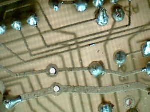
Intel QX3+ Microscope with monitor in background displaying microscope’s view of a copper trace on the homemade circuit board
The microscope is well designed and made from relatively high quality parts. Although there are some software issues and a significant limitation regarding depth of focus (covered at the end of this article), it is an excellent microscope for the price. The most important thing to be aware of is that Intel is no longer making or selling microscopes, so bug fixes, repairs, upgrades, and new models won’t be coming.
The microscope can take still pictures, movies, as well as stop-action movies (one frame every x seconds/hours/days).
Motorola logo on a chip at 10x, 60x, and 200x magnification
The microscope has three zoom levels: 10x, 60x, and 200x. (Actually, Intel cheated a bit. Because each pixel on the monitor is larger than each pixel on the microscope’s camera, a majority of the magnification comes from the camera-to-monitor pixel size difference. Regardless, the technique is ingenious and perfectly effective.)
At 200x, material texture and details that aren’t apparent to the naked eye are easily discerned.

Left: PCB at 10x magnification, lit from above. Right: Same, but lit from below (plus room lighting from above).
As would be expected, lighting plays a key role in determining what is seen. The microscope comes with two light sources; one above and one below. When lit from above, the top surface details are apparent. When a semi-transparent specimen is lit from below, a blend of surfaces and internal details results.
For example, if you’re interested in inspecting the cleanliness of the top surface, light it from above. If you’re interested in seeing how well the traces on both sides of a circuit board converge, light it from below.
In all cases, external room lighting can be beneficial in improving image quality. In fact, by moving the position of an external light source, the changing shadows and reflections enhance various characteristics of the specimen.
The bulbs included with the microscope can take 15 minutes to reach their maximum intensity. Therefore, it is worth leaving the microscope turned on if you plan to continue using it, rather than turning the microscope on and off every five minutes.

Thin, light-colored (and tiny) circuit board placed on black construction paper
Another useful lighting trick is to place a piece of black construction paper underneath light-colored or thin specimens to improve contrast, assuming you’re not planning to light the specimens from below.

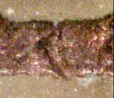
Copper trace at 60x and 200x, showing the effect of pixel steps
The software I use for creating PCBs uses a patterned background to prevent direct printouts. The company wants people to order boards through them (which I also do), rather than making your own at home.
To get around that, I take screen shots of my circuits and then print them from a paint program. The downside to this approach is that the screen resolution (say 72 dpi - dots per inch) is much less dense than a direct printout (say 600 dpi). Although, depending on how far zoomed-in the circuit is before taking a screen shot, the resulting dpi can be increased significantly. It’s just a pain to reassemble the screen shots before printing.
I didn’t think too much about the dpi problem until I viewed a homemade PCB under the microscope. A diagonal copper trace showed significant aliasing, also known as staircasing or jaggies. You can see how a single screen pixel shift horizontally ended up being quite large on the final etched circuit board.
Aside, but also of interest, the 200x magnified view shows the depth/thickness of the copper trace.

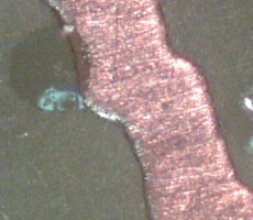
The letters 'kH', showing partial transfer and a crack
During circuit board inspections with the microscope, careful attention was paid to the smallest traces and to the edges of the board.
Obviously thinner lines are more susceptible to scratches and breaks in the copper. They’re also more susceptible to undercutting, that is, the etchant digging underneath the protective resist.
The edges of the board don’t receive the same amount of coverage and pressure during pre-cleaning of the board, so the oxides and grime may not be removed as effectively, which prevents a clean transfer. Nor do the edges receive the same heat and pressure during ironing, as does the center portion of the board, again affecting transfer.
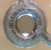
On one example circuit board, I ran across the letters 'k' and 'H' from the word “kHz”. The 'k' suffered from either an incomplete transfer during ironing (likely) or being scrubbed off during post-etching cleaning (possible, but less likely). It’s interesting to see that it isn’t a clean snap-off, but more of a smooth fade in the copper.
The letter 'H' (about 1 millimeter wide) has a crack in the middle of it. At 200x magnification, the crack is quite apparent. Testing with the continuity mode of a multimeter indicates that the crack doesn’t completely break electrically. However, this crack would affect the maximum current carrying capability if it were in a circuit trace. Since this was probably a flaw in the original copper board, this demonstrates a good reason to use as large as possible traces on your homemade boards.
In no case did I find any evidence of undercutting. The edges of the copper appear nicely rounded and smooth.


Cleanly and poorly drilled holes in PCB at 60x magnification. Rightmost image shows PCB fibers
Examination of the home-drilled holes shows remarkable differences. In the cases pictured above, the same #66 drill bit (0.033 inches) produced radically different quality holes. At 200x magnification, the splintering of the fibers in the PCB substrate is quite noticeable.
Professional PCB hole at 60x magnification
Compare that with the crispness of a hole of approximately the same size from a professionally manufactured PCB.
On the professional PCB hole, notice that the inside of the hole is plated through to the other side. Through-hole plating electrically connects the front to the back side of the board, as well as increases electrical contact area with any wire or component inserted, as well as allows the component to be soldered to either side of the board (since both sides electrically connected either way).
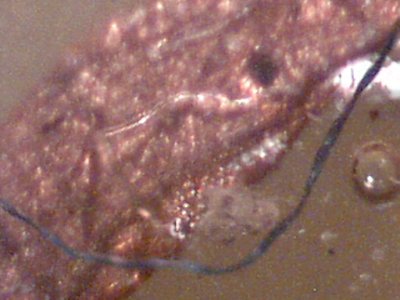
Residue from flux paste and attracted debris at 200x magnification
I readily admit that my robot laboratory wouldn’t qualify as a “clean room”, even on its best days. Still, I was a little shocked when I ran across the above bad neighborhood on my homemade circuit board.
I believe the board had been cleaned in an ultrasonic cleaner with isopropyl alcohol. Apparently a different kind of cleaning solution is necessary to remove flux paste residue. The sticky paste tends to collect microscopic debris, in this case a tiny dust bunny and a blue thread.
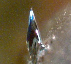
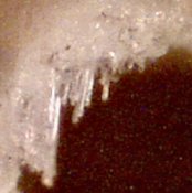
A spur coming off a solder connection. 200x magnification
One of the tasks I hoped to perform with the microscope was to be able to carefully examine the quality of my soldering. In some cases, the microscope revealed very interesting anomalies, such as the solder spur (soldercicle?), in crisp detail. Removing the solder from the solder joint after removing the soldering iron, instead of before, probably created the spur.
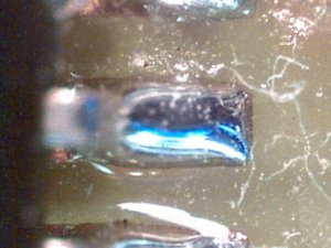
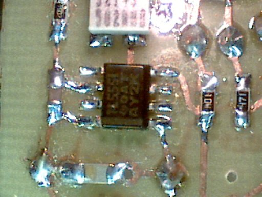
Unable to sharply focus on both the printed circuit board pads and the raised solder details at the same time
Unfortunately, the microscope does not have an incredible depth of focus. In other words, it isn’t possible to clearly examine both near and far details simultaneously. For example, even the pins and solder pads of even a fairly flat SOIC chip can’t be seen in focus at the same time.
The lack of focus depth makes rapid examination of the soldering of the finished board very difficult, if not impossible. You’re constantly focusing in and out to get a sense for the quality of a connection.
Full size view as is seen in the microscope’s software. Notice the visibility problems with focus and lighting.
The above image has not been scaled or retouched. This is the full size and quality of the circuit board image at 10x magnification. This demonstrates the difficulty of rapidly examining a board for errors.
The included software is very good, but suffers from a few flaws. The biggest problem is that the software doesn’t share the screen with other applications. It forces to monitor to 800 x 600 mode and prevents access to other applications while it is running.
Additionally, the software has some minor bugs. For example, when trying to export images, most (but not all) refused to save as jpgs. By choosing to save as bitmaps (.bmp) instead, the microscope’s software was able to export all of them. You can then use a proper paint program to resize, crop, and convert to jpg.
At times the machine slowed to a crawl. This was with a 2.26 GHz Pentium 4, 1 GB RAM, 120 GB 7200 RPM hard drive, USB 2.0, and ATI 7500 Radeon video card. So, no hardware excuses there.
If you’ve got the time to fiddle with lighting and focus, the Intel QX3+ microscope is a wonderful tool for exploring circuit boards. It’s a shame that Intel felt it was unable to profitably continue the line. I can only imagine the inexpensive, yet more powerful microscopes that were to have come.
Besides circuit board inspection, the microscope also provides at least an afternoon of bonding time with your children. The bugs, flowers, dirt, and seeds of our modest garden revealed their secrets in vibrant splendor.
Fifteen years later, I compared these microscopic images to a 16 MP camera with a macro lens. Was the modern camera able to out-magnify the old microscope?