

Previously, we looked at cutting and cleaning copper clad for making homemade PCBs. Now, we’re going to look at the best conditions to iron Press-N-Peel film to transfer laser printer toner to the copper clad boards.
Each board was sanded, washed, and then treated before applying the circuit design. The film and copper board were initially covered by a piece of paper to prevent the film from slipping until the heat partially adhered the film to the board. The iron was allowed to fully reach the temperature on the dial before beginning. Ironing occurred on a flat table with a flat wooden board to prevent the board from bowing.
Here are the results:
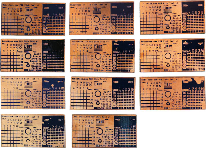
PCB transfer film failures
I won’t bother the list all of the variations of pressure, temperature, and time, because none of the boards are acceptable. Each board suffers from bare spots, smearing/spreading, or both.
For example, this board has gaps in the fonts and lines:

Uneven pressure and slightly too much heat
This board has speckled bare spots, and the letters and lines have swelled together.

Too much heat and pressure
Using a FLIR infrared camera, you can see how uneven the heat is on my household iron. (My wife kept shouting “Use the 'good' iron”.)


Infrared image of uneven heating of household iron
There is over a 150 degree difference in temperature on the bottom of the iron. This is particularly problematic if you try to iron with just the tip, as it doesn’t reach the dial temperature.
Well, at least the iron is flat. Certainly if you apply force to the middle of the handle it will spread out across the board? Nope. Check out the pattern on the paper cover:

Uneven pressure when ironing PCB transfer
Residue from the iron is deposited unevenly, indicating that the surface of the iron and the surface of the paper are not uniform enough. They are making contact at particular high spots, likely leaving bare spots in the toner at the low spots.
Rigidity and relative lack of flatness results in uneven pressure and uneven application of heat. I suppose this is why so many hobbyists have turned to laminating machines with rubber pinch rollers. The rubber has enough flexibility to conform to the mating surface.
I tried using a cover of aluminum foil, instead of paper, because aluminum has better thermal characteristics and will shape itself to the pattern on the transfer film. Indeed, it works better, but an aluminum foil pouch was not the critical key to perfecting the process.
After so many disappointing boards, I spent time on the interwebs to see if anyone had any other variations to try. I found the solution at PCB Fab In A Box. They suggest that you want to find a temperature where the laser toner become tacky or sticky, but has not melted. In doing so, the toner will adhere to the copper board without distorting under pressure.
Here is a successful process:
Depending on the size of the board and the material used in your laser printer’s toner, you may need to make adjustments to time and temperature. However, I strongly agree with the PCB Fab In A Box theory that the toner has a state where it is sticky but less prone to spreading. Finding this sweet spot allows you the time to work the entire board to avoid bare spots, without the concern of distortion.
The low temperature also has the benefit of supporting double-sided boards. You don’t need to worry about overheating when you flip the board over to work the other side.
Here is the result:

Good result of transferring toner to copper clad board
(Yes, I wish I had used a better cut board. Yes, I wish I had centered the film better before ironing. Yes, I wish I had treated the board to clean it better. But, up to this point, I had so many failures that I wasn’t putting the effort into it anymore.)
This low-temperature thermal toner transfer technique is great. There are some small imperfections, which I’ll look at in more detail on the next page. However, this is far superior to all of my previous attempts.
I etched the board using a sponge and ferric chloride. I like this method because it uses less etchant and can be applied where needed to reduce overetching and underetching.
The results are terrific. Even tiny details, like a font with 7 thou (7 mil, 0.007 inch, 0.17 mm) lines is crisp and legible.

Quality of fonts on home etched PCB
Holes as small as 8 thou (8 mil, 0.008 inch, 0.20 mm) are usable. Traces down to 6 thou (6 mil, 0.006 inch, 0.15 mm) are unbroken.

Home etching 6 thou PCB
In the above image, the thickness of 7 thou and 8 thou traces seems identical. Why?
I have a 600 DPI printer. It is capable of producing dots down to 1/600 (0.00166) inch. A 0.007 trace is 0.007/0.00166 or 4.2 dots. The printer cannot create partial dots. So, the trace is 4 printer dots.
A 0.008 trace is 0.008/0.00166 or 4.6 dots. Assuming this is calculated as an integer, then that’s 4 printer dots -- the same as the 0.007 trace.
Instead, imagine they rounded 0.008 up to 5 printer dots. Well, since 0.009/0.00166 = 5.4 dots, then a 0.008 trace would be identical to a 0.009 trace. Sooner or later, you’re going to have traces that have the same width if the resolution of the printer isn’t small enough.
The printer DPI is a significant quality factor when producing PCBs with such small details. At this point, I wish I had a 1200 DPI laser printer. (Are you listening Dell, Brother, and HP?)
Clearance in large copper fills works well for straight lines. The results are acceptable for curvy areas with a clearance of at least 10 thou (10 mil, 0.010 inch, 0.25 mm). However, narrow curvy areas (such as around fonts) with less than 10 thou clearance tend to get filled by either rendering, DPI, or Press-N-Peel fill issues.

Clearance on home etched PCB
Here is the full home-etched board:

Nicely etched PCB using toner transfer method
As pleased as I am with the results, the quality doesn't match a professionally manufactured PCB, particularly with the tiny pads at the middle bottom and the clearance around the 6 on the upper right. Below is the same circuit board test pattern reproduced by OSH Park.

OSH Park example board quality
If you want to try this yourself, remember that most manufactured boards place solder mask over all exposed copper except for the pads. My test design adds keep out pours to the top and bottom solder mask to ensure I can see all of the copper.
I learned that lower heat produces higher-quality toner-transfer PCB boards. There are still a few minor issues that we need to look at in closer detail, to determine the cause.