Integrated-circuit (IC) manufacturers produce fewer new designs in dual in-line package (DIP), shrink dual in-line package (SDIP), or other through-hole forms. These are the classic looking chips that have legs that extend through the circuit board and are soldered on the other side. They’re easy to put into sockets and easy to use on solderless breadboards.
Most of the new families appear only in surface-mount technology (SMT), surface mount device (Philips SMD), or surface mount component (SMC) packaging such as small outline integrated circuit (SOIC), small outline J-leaded (SOJ), small outline transistor (SOT), plastic leaded chip carrier (PLCC), quad flat pack (QFP), or thin small outline package (TSOP). Without special adapter (carrier) boards, surface-mounted components make breadboarding and hobbyist experimentation difficult.
However, Mario Becroft demonstrates that surface mounting isn’t beyond hand-soldering tools. His work challenged me to attempt SMT components myself.
Although ultimately successful, the initial learning process was slow and painstaking. The reward is a lighter (sometimes smaller) board with advanced CMOS technology. In this case, a pair of AC299s can drive higher-current loads (25 mA), which allows my microcontroller to individually enable 16 LEDs via a serial line.
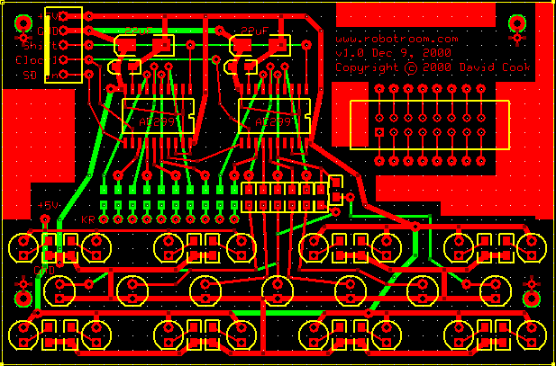
Computer-aided design image created in free software
The circuit image is created using the same technique as the double-sided PCB, but with SMT-component outlines included from the CAD software’s library. Missing component sizes can be made with rectangles and lines from the standard drawing tools.
A problem immediately apparent was the lack of space in-between chip leads, so a lot more lines needed to be routed under to the lower layer. I suspect these chips really only save space in boards with more than two layers!
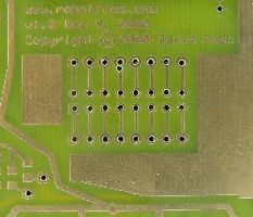
Unetched rectangles of copper
To save etchant, large unused areas of the board were designed to retain copper. This also stiffens the board a bit but adds a tiny amount of weight. It also significantly improves thermal performance and reduces electrical noise. Nicer CAD programs can automatically fill-in all the irregular areas or turn them into ground plains.
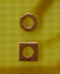
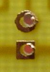
Left: The top layer isn’t correctly positioned directly over the bottom layer. Right: The poor alignment means the holes don’t drill well from one side to the other.
Thinking I was an expert, I got sloppy drilling the alignment holes in the corners of the board. This resulted in poor registration of the top and bottom layers, especially towards one corner of the board. In the picture to the left, notice the circle on the top layer isn’t directly overhead the faint circle at the end of the trace line on the bottom layer.
Even though the via holes aren’t directly over each other like they should be, the alignment isn’t so bad that the board is unusable. However, when a hole is drilled in the center of a circle on one layer, it ends up off center on the other side, ripping out some of the copper pattern. In the picture to the right, the off-center holes are actually perfectly centered on the other side of the board.
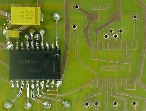
A SOIC package mounted on pads
Using standard solder and my usual fine-tip soldering iron, the SOIC packaged IC connected easily to the pads. It helps to solder one pin on one side and then solder a pin on the opposite corner and then all of the other pins. To prevent solder from bridging between pins, draw the excess solder back onto the copper traces.
The surface-mounted capacitors (yellow rectangles in the upper-left) were more difficult to connect, as they had a habit of sliding out of alignment. Unlike through-hole varieties, the layer beneath the surface-mounted components is available for traces or other components.
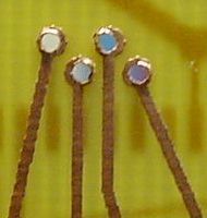
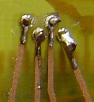
Left: Four holes too close together with too thin of pad circles. Right: Difficult soldering leads to bad connections and possible bridges
I tried to save space on some of the via holes by using the same density as professionally-manufactured boards. That was a mistake. I don’t have accurate enough tools (or eyes) to drill and solder holes with such tight spacing. Before taking this picture, it appeared to me that the solder job was adequate, but now magnified I think it looks like *#^%!
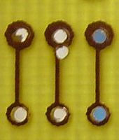
You didn’t want a hole there?
The third hole in the center was a significant miss of the drill bit. Apparently I was sleepy. The almost-broken trace was corrected by making the errant hole a via by passing bare wire through the hole and soldering both sides.
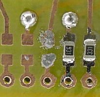
Solder paste for attaching resistors
The surface-mounted resistors ended up being too much trouble to use except in a space pinch. I tried gluing them on before soldering, but neither super glue nor Elmer’s nor tacky glue held them (later on I discovered that silicone glue works great). Finally, I used a little solder paste on each pad, positioned the resistors with tweezers, and heated the copper traces with the tip of a soldering iron.
Solder paste consists of microscopic balls of solder suspended in a flux paste. It comes in syringe dispensers. The paste needs to be kept cool to prevent from drying out or melting together, so it is usually only available from catalog companies with overnight delivery.
I don’t recommend solder paste. It works well for production boards when applied with a screen template. However, it doesn’t seem the best choice for manual operations.
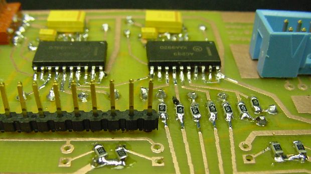
Completed double-sided PCB with surface-mounted resistors, logic chips, and capacitors
The completed board is double-sided with surface-mounted resistors (foreground), SOIC logic chips (middle), and capacitors (background). Although most of the resistors soldered straight, a few are askew. The solder looks like a mess when magnified, but it’s the best I can do with my tools and experience.
It turns out some advice (below), a lot of practice, and some silicone glue helps a lot! For the continuing story, see Infrared Revisited.
It looks like you had fairly good results through using the toner transfer system. I was using a photographic process and could do tracks down to 12 mils if I was careful. But it was difficult and fault-prone. For a while I used a plotter to draw the pattern onto film, but later I used a laser printer. No doubt if I had better equipment it would have been easier.
Now about surface-mount soldering: Trust me, it’s very easy once you get the hang of it. I use surface mount chips and discretes by choice now because I can solder them faster than through hole parts (when you count the time taken to cut leads on through hole resistors etc), and they are smaller.
For resistors and capacitors: try to use 1206 parts if you can, since they are easier to hold. Forget solder paste. Simply put a small blob of solder onto ONE pad of each part. Only a tiny amount of solder is required, just enough to make a slightly raised surface over the pad. For each SMD part: position it, and while pressing down from above with one hand, melt the solder. When the part has sunk into the solder, remove the heat. Having done this, solder the other side of each part. Sometimes the first side needs touching up if it didn’t flow well. You need very little solder! Using this method, the parts should not move around. You can use a fingernail to push down on the part as you melt the first pad, or if your finger is getting too hot, you could use a thin stick or screwdriver. If you find the parts hard to handle, you could try tweezers, but a better method is a thin wooden stick like a skewer, with “blu-tack” (semi-adhesive gummy material used for sticking pictures on the wall etc.) on the end. This sticks to the part and lets you position it very easily.
For chips, it sounds like you have the right idea. Tack two corners first to hold it in place. Solder bridging between pins is not an issue. You don’t even have to solder each pin individually. Just run the soldering iron along the pins while applying solder. You can solder pins one at a time or in groups of 2 or 3, which can be better especially with wide pitch pins like SOIC. Solder bridges will occur - just run over the pins with solder wick to remove the excess solder. You have to put on excess solder to make it flow properly. A better way is to get a tube of flux. Apply generous amounts of flux to the pins before soldering. This way you don’t need to apply excess solder, and if you are careful, there will be no excess to remove.
There is no problem with solder bridging between pins. You can get excess solder, but this doesn’t matter. As long as there is enough flux, the solder will automatically flow away from the gaps between pins. If the solder is not flowing this is because of insufficient flux, and you must add more solder or liquid flux. Paradoxically, this means that if there is a solder bridging, adding solder can sometimes remove the bridge! Whenever you have excess solder, simply remove it with solder wick. Admittedly solder mask and metallised pad surfaces does make this a little easier, but it’s not a big deal.
With this method you will have no trouble soldering a GP32. When you get to very fine pins (0.5 mm - much finer than the GP32) it can be a little bit tricky, but the same techniques apply, you just have to be extra careful not to bend the pins, and sometimes a scalpel is needed to dislodge solder from stubborn places. But when you’re doing pins above 0.8 mm pitch, none of this is necessary.
I can solder a GP32 in 30 seconds, all going well, using the above method. That’s better than one pin per second. Realistically it can take 1 minute when there are a few solder bridges to remove and such like.
Never in any of this do you need glue to hold parts in place! This is completely unnecessary and just makes things slow and difficult.
For an example of very fine-pitch soldering, have a look at http://gem.win.co.nz/mario/hardware/galaxy.html
I hand-soldered soldered the 208-pin QFP (0.5 mm lead pitch) on that board using the methods described above. I think it may have taken a quarter of an hour or thereabouts.
Now here’s my soldering problem: how to solder BGA packages! It’s pretty obvious that hand soldering these is impossible, but I wonder if there is some sort of hot-air process that can be used at home. (Or maybe even a crude reflow process in a domestic oven??)
It’s not ball grid array (BGA), but here’s a link to an oven in action: http://www.seattlerobotics.org/encoder/200006/oven_art.htm
Over the years, I’ve gotten much better at SMT soldering than this page may seem to indicate. For homemade circuit boards, I now prefer SMT components because I don’t have to drill holes for them.
Contrary to other opinions, I still like to use silicone glue to hold the SMDs to the board before soldering. Maybe I just don’t have as steady a hand or tolerance for heat as other people?
You don’t need a needle-like applicator for applying flux. In fact, you can douse the flux and solder quite liberally onto a multi-pin part like a chip. After applying a blob of flux, heat each pin with the solder wire touching the pin (this causes the flux to activate, the solder to melt, and the solder to wick onto pins and traces). If too much solder remains, draw the soldering iron tip between pins to drag the solder out onto traces. If there’s still too much solder, use a solder sucker.
Common sense would have you believe that you need to be really precise with solder and flux on tiny little pins. It just doesn’t turn out to be the case. In fact, modern manufacturing processes for SMT can involve waves of molten solder grossly flowing over the entire board (or vapor solder collecting like dew). The solder clings to clean metal, but not to PCB substrate or plastic packaging.